True 3D AOIs to Improve Production Quality
By Joseph Park, Senior Application Engineer and Denis Kang, Senior Sales Manager, Koh Young Technology
3D Automated Optical Inspection (AOI) systems have become an integral solution for the surface-mount technology (SMT) industry. These systems have become more important for manufacturers, because they provide incomparable reliability to help maintain high quality of boards with thousands of solder joints. However, does this mean every 3D AOI can be the ultimate gatekeeper to identify defects early in the process? The answer may be both yes and no. Due to increasing component miniaturization, optical inspection systems face many physical limitations, which true 3D-based systems must overcome. Koh Young Technology, the leading true 3D measurement and inspection solution provider, intelligently combines 2D and 3D technologies to overcome these limitations and provide superior results.
2D versus 3D AOI Systems
When we look at the optical inspection market growth trajectory, we can see how unsolved difficulties help create innovations. Solder Paste Inspection (SPI) has undergone a shift from 2D to 3D, because 2D technologies that were used to collect a solder deposit image could not solve shadow problems. Likewise, Koh Young developed 3D SPI to capture the printed solder paste height to accurately measure the total volume of paste printed. Several years later, we see the same need for component inspection with AOI systems. As today’s board complexity is increasing with more components, more joints, higher density, and new package technologies such as 01005 size and even 008004 size microchips, 2D AOI technology using grey-scale image analysis or angled camera view of color images may no longer be a viable option. Most decisions made based on “good-bad” comparison of reference images, which can easily be affected by variables like component surface finish, board condition, component proximity, and more.
Although 2D AOI is still a major technology in the market, more manufacturers are adopting 3D AOI to increase board quality. The benefits are clear: putting rock-solid faith in inspection tolerances and reducing efforts to constantly debug inspection programs. Moreover, measurement data generated from 3D AOIs provides meaningful insights about the process and helps eliminate the root causes of a defect. The 3D SPI, together with 3D AOI, enables manufacturers to accurately control and monitor the solder printing and component placement processes. What are the requirements of 3D AOIs to go from inspection to measurement, and ultimately to process control and optimization? Simply put, 3D AOIs must fulfill three “Rs” for measurement data: reliable, repeatable, and relatable. Koh Young, as the pioneer in 3D technologies, intelligently combines 2D and 3D technologies to offer the best inspection and generate meaningful data; which satisfy three “Rs.”
Full 3D Inspection
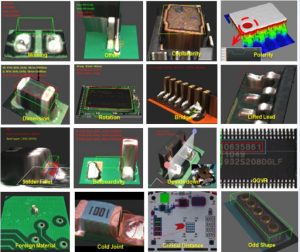
Current AOI vendors offer a limited level of 3D coverage for components and solder joints. Koh Young, which defined complete 3D inspection more than 15 years, provides full 3D coverage to identify boards with defects and help manufacturers monitor their performance. Their 3D AOI systems not only inspects common defects like missing or wrong components, but accurately identifies coplanarity and lead bridging issue; which are prevalent in small packages and BGAs. (Figure 1) The 3D AOI solutions from Koh Young uses a patented multi-frequency shadow Moiré technology to measure the z-axis profilometry of the entire board. By measuring components and solder joints, and then offering critical height information to the inspection algorithms, manufacturers can identify errors like pad overhang and insufficient solder. Unlike 3D AOI systems using a brightness threshold, the Koh Young’s Zenith 3D AOI uses the height threshold to extract critical body and the lead tip information. This data allows the Zenith 3D AOI to provide reliable body and joint measurements with CAD dimensions, since it can locate body properly in the very first stage of inspection process.
Figure 1: Koh Young Full 3D Inspection Coverage
Shadow Problems
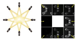
Will accurate body-finding guarantee accurate 3D measurement data? Not necessarily. There are several inspection challenges even with high quality 3D inspection. One major problem is the shadow effect. When various components are assembled on a board, some short parts like resistors may be shadowed by tall neighboring components like connectors, which leads to inaccurate 3D measurement results. By using 8-way projection, Koh Young eliminates blind spots and can construct a true 3D image using the multiple projections available. (Figure 2)
Figure 2: Koh Young’s 8-way projection to overcome shadow problem
Inter-reflection Problem
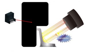
Another critical issue is inter-reflection. The soldered and tinned components on assembled boards may have specular surfaces, which will reflect some lighting back to camera, while creating strong inter-reflection with other lighting reflections. (Figure 3) Since some of the reflected light does not reach the camera, they generate false signals that cause height measurement value corruption. This specular reflection issue is becoming more troublesome, as board density is increasing and component spacing is decreasing. The Koh Young Zenith AOI overcomes this with its superior multi-view sensors and eliminates measurement inaccuracies with advanced 3D image fusion algorithm. The Zenith 3D AOI meticulously identifies and filters the multiple reflections caused by shiny components and reflective solder joints with multi-projections and intelligent algorithms.
Figure 3: Single projection’s problem with specular areas
Solder Joints
When it comes to solder joint measurement, it is much more complicated than a component body, because the solder deposit varies depending on board design, printing conditions, and they have specular reflections. Such differences can affect the optical inspection of defective solder joints. To help, Koh Young has developed an algorithm that is applied to the data and generates robust and stable measurement data for resistor, capacitor, and other component leads, regardless of solder joint quantity or shape. (Figure 4) Moreover, the Zenith 3D AOI helps to verify solder joint quality with measurement conditions adhering the various IPC-610 standards. IPC-610 standards describe to satisfy quality class 3, a barrel fill of 75% is required, which translates into z-dimension with 3D algorithm. However, due to specular reflections of solder joints, only true 3D inspection could offer reliable solder joint results. (Figure 5)
Figure 4: Koh Young’s 3D solder joint measurement example
Board Warpage
Figure 5. Zenith’s Solder Joint Inspection under IPC-610 Standard
Board warp also creates a challenge for 3D inspection. On a warp board, pad positions defined by board CAD or Gerber files appear distorted; thus, confusing conventional inspection systems and generating incorrect data. Board warp becomes more pronounced during the reflow process due to high temperatures required for processing. The board warp results in different height levels for the same component due to the variable base plane difference – even when using high quality components. Therefore, Koh Young established a strong algorithm to actively compensate for warpage with advanced algorithms.
Speed and inspection consistency
Another limitation associated with 3D optical inspection systems is the cycle time typically associated with processing millions of pixels to reconstruct a full 3D images using new data captured from multiple channels. Koh Young does not compromise 3D measurement for throughput. Despite capturing up to 32 unique measurement data sets for each field of view, 15-years know how in 3D big data processing and its parallel computing hardware ensures the throughput will satisfy the most demanding applications.
Koh Young further improves 3D AOI speed. The company’s Zenith AOI has superior hardware and industry-leading optical technology that generates reliable and repeatable data. These inspection results are then will be stored in central database, which can be used in deploying optimal program for multiple operations and reducing programming and setting condition times.
Process optimization with reliable data
Process optimization is desired by every manufacturer, as well as equipment suppliers, including automated inspection providers. However, it has been difficult to be achieved for 2D AOI systems, as they do not offer height information and it is impossible to accurately measure and quantify shape, coplanarity, solder amount. Koh Young 3D AOI systems overcome these challenges by measuring every aspect of the component and solder joint in accordance with the IPC-610 standard and generate a significant set of reliable measurement data.
These data are stored and processed in newly developed smart factory solution suite called KSMART, where it will be help users with dynamic decision making. Comprised of multiple modules, performance monitoring modules like RTM@KSMART (Real-time Monitoring) and Link@KSMART helps the real-time monitoring of line performance with highest transparency, while KPO (KSMART Process Optimizer) modules can even optimize the printing process by recommending optimal printing parameters.
Conclusion
Nowadays, boards are becoming more complex with increasing component miniaturization. The challenges and limitations of optical inspection systems can no longer be overlooked, because they can be the cause for false calls and escapes. 3D AOI systems, one of the latest technologies to identify defective boards, are not exempt. Manufacturers need to think twice when suppliers claim 3D inspection – is it modified 2D or full 3D measurement capability? Koh Young, the leading 3D measurement-based inspection and solutions provider, overcomes these challenges by intelligently combining technologies with superior hardware to provide true 3D optical inspection solutions and ultimately improve manufacturer’s process.


