Silicon Wafer Suppliers May Need to Start Greenfield Investments to Meet Growing Demand

Originally posted on SEMI Blog
After logging record shipments in the first quarter of 2021, the silicon wafer industry may need to start greenfield projects as soon as this year to boost capacity over the next two years as market demand and average selling prices continue to improve.
One segment hamstrung by a supply shortage is 300mm epitaxial wafers, a shortfall we expect to drive continuing price increases in the coming quarters. In a countertrend, the 300mm polished wafer segment still has some inventory leeway with current reserves in the supply chain, though the recent surge in memory demand will drive a polished wafer recovery that draws down that surplus. Memory makers will then increase investments in capacity to meet rising demand after the soft 2019 followed by the pandemic-ridden 2020 – two years during which they added little new capacity. Historically, memory pricing trends, specifically DRAM ASP, have been strongly correlated with the overall silicon wafer ASP (Figure 1).

Figure 1. Year-over-year growth rate comparison between DRAM ASP and Silicon wafer ASP
While DRAM pricing has been rising since the first quarter of 2021 after bottoming out, the NAND flash market is not far behind with pricing projected to start improving in the second quarter. Recent earnings announcements by memory makers have also pointed to robust demand for memory overall in the coming quarters, with healthy pricing for both DRAM and NAND flash expected to drive additional memory capacity increases in the second half of 2021 and into 2022. Growing demand for 300mm polished wafers could worsen the ongoing 300mm epitaxial wafer shortage.
Although demand is rebounding faster than expected, some silicon wafer suppliers may not be ready for the market boom. With the drop in prices that began in 2019, many wafer suppliers have not made greenfield investments despite the long-term agreements (LTAs) meant to stabilize pricing – dynamics that are about to change. Semiconductor fab construction spending in 2021 and 2022 is forecast to surpass the previous peak in 2018 and 2019 (Figure 2). These future fabs will become the primary driver for 300mm silicon wafer market growth over the next few years. However, limited cleanroom space will be a headwind to significant capacity expansions at existing silicon wafer factories. The upshot is that the balance between supply and demand could tilt toward shortages because of the disparity between the pace of device makers’ capacity investments and wafer suppliers’ greenfield spending.

Figure 2. 300mm semiconductor fab construction spending forecast
If wafer suppliers add no new cleanroom space within the next two years, the wafer market will face a shortage similar to the one in 2017 to 2018, forcing some suppliers to finalize investment plans for new greenfield projects or start construction no later than this year. For their part, chipmakers, especially foundry and memory companies, may need to put in place additional LTAs for newly constructed fabs in 2021. To meet growing demand, some chipmakers will form strategic partnerships with wafer companies that are competitive in both scale and technological ability.
In the short term, with the expected increase in demand for memory, the supply and demand balance for 300mm polished wafers will tighten entering the second half of 2021. However, if IC and component shortages for automotive, mobile phone, networking, GPU, and data center devices continue through 2021, the shortfalls will hamper overall memory demand in these vertical markets, potentially slowing the growth of the 300mm polished wafer market. Another risk is the lead time for capital equipment delivery may be extended, as SK Hynix mentioned in its most recent earnings call. Longer equipment delivery times for both foundry and memory fabs could slow capacity ramp-ups scheduled for the coming quarters.
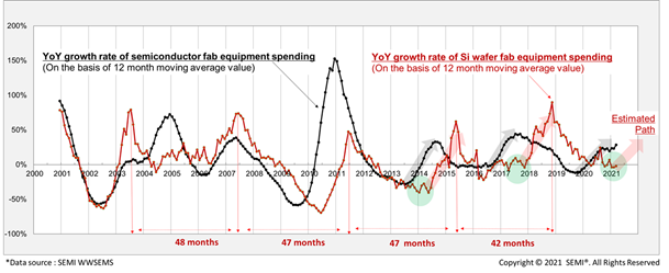
The big takeaway is that wafer manufacturing equipment spending is projected to increase (Figure 3) as some wafer suppliers expand 300mm epitaxial wafer capacity this year as part of brownfield investments – momentum that will continue as some wafer suppliers start preparing for new cleanroom space made possible by greenfield projects.

Figure 3. Equipment spending comparison between semiconductor fabs and wafer production facilities
For more information about silicon wafer market dynamics, please refer to the SEMI Silicon Wafer Market Monitor report.
Sungho Yoon is senior manager, Industry Research & Statistics, at SEMI.


