SEMI Europe and ESIA Drive Positive Outcomes Through PFAS Advocacy
By Stefano Orlando, SEMI
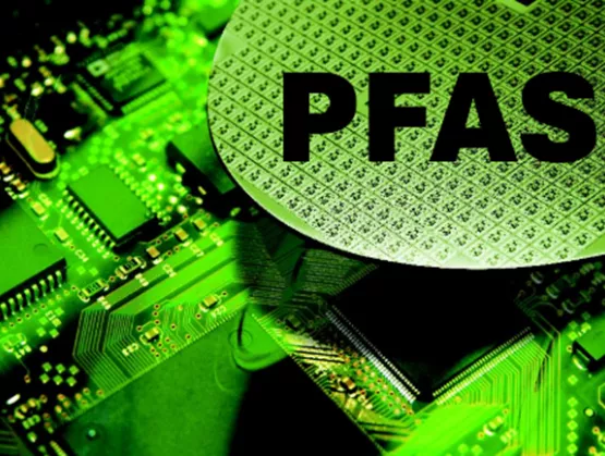
Per- and polyfluoroalkyl substances (PFAS) are a large class of thousands of synthetic chemicals that are used throughout the semiconductor industry in the form of gases, liquids, and solid high-molecular weight polymers, due to their wide range of physical and chemical properties. PFAS contain carbon-fluorine bonds, which are one of the strongest chemical bonds in organic chemistry, allowing them to resist degradation and to cover long distances away from the source of their release.
In recent years, the high persistence of PFAS in both the environment and the human body has encouraged the European Chemicals Agency (ECHA) to launch a PFAS restriction proposal aiming to regulate and eliminate their use over the next few years. The proposal is currently under assessment by ECHA’s scientific committees for Risk Assessment (RAC) and for Socio-Economic Analysis (SEAC).
PFAS in the Semiconductor Industry
The exceptional physiochemical properties of PFAS provide them a high degree of functionality in semiconductor manufacturing across the entire supply chain, and often the combination of their properties allows manufacturers to satisfy multiple and overlapping technical requirements.
While the industry recognizes the importance of transitioning away from PFAS, and research to that effect is ongoing, current technological limitations do not allow the industry to manufacture semiconductors without the use of PFAS or to discover scientifically viable alternatives that can effectively substitute their use.
At this point in time, no known alternatives exist for most of the uses of PFAS by the semiconductor industry. Alternative substances must be researched, invented and potentially applied into mass production to be recognized as viable alternatives. Many different pathways will have to be explored as PFAS are currently used across the entire supply chain for over 1,000 semiconductor applications, including articles, support equipment and fab operations, or as process chemicals.
SEMI Europe—European Semiconductor Industry Association (ESIA) PFAS Research Workshop
Considering the criticality of the PFAS issue for the semiconductor industry, SEMI and the European Semiconductor Industry Association (ESIA) have greatly strengthened their joint advocacy efforts over this past year concerning the ECHA’s PFAS restriction proposal.
In this regard, SEMI and ESIA successfully organized a workshop in October 2023 with the relevant representatives of the European Commission (DG GROW, DG ENV, DG CNECT and DG RTD) to present and discuss in-depth the key technical evidence for the use of PFAS is the semiconductor sector. The discussions built upon the extensive technical evidence that was presented by SEMI and ESIA in their respective submissions for the six-month PFAS consultation facilitated by ECHA.
Following the successful execution of this first workshop, there was a keen interest from the European Commission to enquire further upon the current state of play of research and development efforts in the field of PFAS detection, abatement, capture and destruction, circularity, recycling and alternatives
For this reason, after the first workshop, ESIA and SEMI collaborated to develop and deploy a joint PFAS Survey aimed at identifying the research priorities in PFAS from the perspective of their member companies.
Based on the survey outcomes, the associations compiled the SEMI–ESIA PFAS Research Roadmap and officially presented it to the representatives of the European Commission during a follow-up workshop on 13th June 2024. Discussions at the workshop focused on the key research priorities for the semiconductor industry to discover potentially viable alternatives to the use of PFAS.
In the upcoming legislative period, SEMI Europe will continue to engage with relevant stakeholders to contribute to the political debate and encourage a legislative framework that can enhance sustainability across industrial supply chains while preserving Europe’s technological competitive advantage.
Get Involved
Get involved in the SEMI PFAS Working Group! The SEMI PFAS Working Group is composed of industry technologists from leading companies across the global semiconductor manufacturing supply chain. The working group meets regularly to share intelligence and develop strategies to earn exemptions and/or extensions from regulators. Join SEMI in this crucial effort to enable the industry to continue manufacturing chips vital to the prosperity of the world by contacting ehs@semi.org.
Stefano Orlando is Manager Advocacy and Public Policy at SEMI Europe.