How to Put “Design” Back into DFT for PCBs
By Mark Laing, Product Marketing Manager, Valor Division, Mentor-A Siemens Business
PCB production and design-for-test (DFT) engineers typically work in different silos with limited communication, making test costly and ineffective. This issue is important particularly for industries where reliability and quality means protecting human life, such as the automotive and medical industries.
Since design for manufacturing (DFM) has become a proactive part of the design process, the same cannot be said for DFT. Whereas “left-shifting” DFM has reduced manufacturing problems, increased yield, reduced scrap levels, and simplified engineering rework, testability-related improvements have remained flat during that same time. Unfortunately, as assembly costs have come down, and test-related costs have remained flat, test now comprises a significant percentage of modern electronics assembly costs.
So should product designers care about test? Reactive considerations for DFT occur too late in the design cycle, resulting in defects that can slip by undetected or require expensive functional test to catch. This results in reduced quality, scrapped boards, and increased costs, which means that product targets are missed, business plans are not met, and bonuses are not paid.
For PCB design, components are typically chosen without looking at their failure rates, and the PCB failure spectrum is large. Test points do not get placed on all the required nets, and BGA devices are selected that have hidden joints. As a result, the opportunity for defects to escape manufacturing test is much higher. Thus, many more defects than necessary have to be found and repaired at the more expensive functional-test stage.
To understand how boards get shipped without visibility to DFT, we need to understand the differences between process and product verification. The former is the ability to determine if a product was built correctly; the latter confirms that it is working to its design specification. Some functional faults can be found during process verification, and a lot of process faults can be found with functional test, but the cost to find and repair those faults is higher.
Process verification includes structural testing, namely solder paste inspection (SPI), automated optical inspection (AOI), automated X-ray inspection (AXI), and electrical test, namely in-circuit test (ICT), boundary scan test (BST), flying probe test (FPT), and manufacturing defects analysis (MDA).
Product verification is usually done through dedicated hardware and software to confirm correct operation through at-speed testing of large parts or the whole board. The process verification techniques isolate individual pins and components and thus, have excellent diagnostics. The result is that a repair engineer can fix process faults more quickly at a lower cost. Functional test will report that failures are across many components, meaning a more trained repair engineer is needed to spend more time to correct the failure. Scrapping boards because of functional failures is therefore, more common. The consequence: missed deadlines and the need to build more boards to make up for those that have been scrapped.
We can see this in Figure 1. As test coverage is suboptimal, the yield at that point is high; but we are not finding enough of the defects that have been caused during assembly at the point where we have good diagnostics and can fix them cost-effectively. Instead, the yield at functional test is low because we are using product verification to find manufacturing process defects.
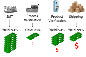
Figure 1: Finding defects as early as possible reduces the cost and improves overall yield. As the product moves further down the process, the costs of fixing defects increases.
Compared to electrical and mechanical engineers, there are fewer test engineers and fewer people are entering the test field. This means that manufacturing and design engineers have to wear more hats, for example, process engineers taking on test engineering responsibilities. This situation, combined with a changing marketplace that has resulted in more products, shorter times to market, higher product mixes, higher variants in products, and lower batch volumes, is unsustainable.
The existing DFT environment needs to change so that DFT and testability analysis is more proactive and works concurrently with the design process. The challenge with considering test analysis at the layout stage is that many design decisions have already been made, opportunities to affect change without causing a knock-on effect is limited, and layout is just naturally sub-optimum for test purposes. So test input must begin at schematic analysis, and then considered as a design constraint just like other mechanical, electrical, and signal and power integrity inputs.
So how can CAD tools work more proactively with test engineering? They have good solutions to place test points already, but because most designs do not have the space to place test points on all nets, we have to determine which nets need test points and which do not—before layout is started. That is, test point requirements should be proactive, not reactive. So how do we know which nets need test points or not?
Let’s look at some places where test points would be typically considered. For physical in-circuit test, test point pitch sizes often are nominally 100, 75, 50, and 39 mil. The lowest cost and most reliable are 100 and 75 mil. The test point pad sizes need to be at least 25-mil diameter, the probe-to-probe spacing the same as probe size, and the probe-to-component spacing half the probe size.
For physical flying probe test points, the targets can be much smaller, typically 10-mil diameter, with no probe-to-probe spacing requirements. Surface mount device (SMD) component pins can be probed, with the offset probe-point away from the component body center.
If we have 100% coverage access, then we have 100% coverage, right? Unfortunately, no. Complete access does not mean full testability. A good example is the small-value bypass capacitors across power rails. They are usually accessible because they have test probes on either side. But they often have large-value capacitors directly in parallel with them, which dominate the measurable result, hence the bypass capacitors are not testable.
So what happens if we cannot achieve 100% coverage because of insufficient PCB real estate or sensitive signals that cannot tolerate the load of a test point? Engineers working on the PCB layout will add test points where they can and not put test points where they cannot. The solution is to get proactive and request test points where we know they are needed. The following are some specific techniques that can help to overcome this lack of access. One of these techniques is using boundary scan.
Test Considerations In the Design Process
For boundary scan test to be supported in an integrated circuit (IC), it must conform to IEEE 1149. The test requires additional circuitry that surrounds the core logic and is controlled with four pins (an optional fifth pin can be included).
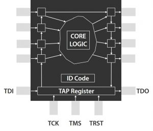
Figure 2: Basic boundary scan layout.
This circuitry allows data to be pushed through a serial bus and out into the nets (Figure 2). Data can also be pushed from the net and captured through another serial bus.
Multiple boundary scan components are typically daisy-chained and controlled through edge connectors, test points, or FPGAs. The chain acts as a single, long-shift register, enabling boundary scan cells to act as virtual drivers/sensors (Figure 3).
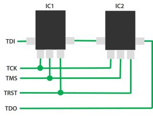
Figure 3: Test access ports are daisy-chained together.
Boundary scan chains must be connected together correctly. If not, they may not operate at all, significantly affecting the ability to test the board. Design tools are not checking the boundary-scan connectivity today, so it is easy for mistakes to be made before the board is fabricated.
Optimizing PCB Layout for Test
DFT analysis must begin at the schematic capture stage—starting with PCB layout is too late. However, even starting DFT at schematic means we still need to actively manage the test point requirements during layout. Test probe access can be achieved through dedicated test points, through-hole component pins, or test vias. Once we have a PCB layout where these physical structures known, this allows us to compare the test-point requirements with the test-point placement. Some nets may be unable to sustain a physical test point on them without risking the design performance. Therefore, on-going DFT and test point analysis is required, both through the initial layout phases, and through subsequent design revisions.
If we see how the typical reactive DFT flow occurs during PCB layout (Figure 4), we find that through the initial revisions, test requirements are not considered. However, at some point, the needs of test must be added and we see a jump in the number of test points on a design. And, as noted, the results will be sub-optimal.
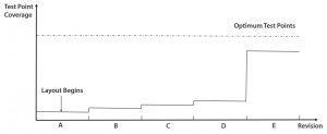
Figure 4: Existing reactive test point management flow.
Comparing this approach with the proactive analysis and actively managed test-point requirements throughout PCB layout, we achieve a higher level of coverage, which enables us to design and build a product at lower cost with higher reliability.
So what are the benefits of PCB designers considering testability in their designs? Many techniques can be used to reduce the requirements for test points across a design, without compromising coverage. Although it may not be possible to include everything that test needs, it is better to make calculated and proactive choices rather than random ones. Further negotiation and communication with test engineers will only improve, as will the overall product quality and cost.
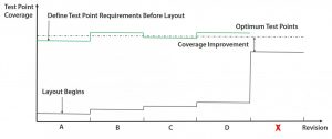
Figure 5: Future reactive test point management flow.
The future of designing PCBs to proactively consider DFT could look like this (Figure 5):
- DFT and testability starts at schematic capture.
- Test point requirements are an input to layout.
- Testability is further managed at layout.
Considering the economics of building and testing today’s PCB designs, we now have the following for process and product verification (Figure 6).
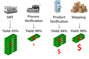
Figure 6: Proactively including DFT in the PCB design stage reduces the costs of finding defects.
Using a proactive DFT strategy, the SMT defect rate is the same and yield is lower at test but much higher at functional test. Failing boards are fixed more quickly and boards are less likely to be scrapped. This change in strategy could result in significant cost savings through the process from PCB design to shipping the final product to customers.
Mark graduated with a B.Sc. in Electrical and Electronic Engineering from Loughborough University, in the UK. He has over 25 years of experience in PCB manufacturing with particular strengths in test and inspection methodologies with three test companies, namely Marconi Instruments in the UK, followed by GenRad and Teradyne in the US.


