Demonstrating How to Reduce Voids in Solder Joints on Land Grid Arrays
Not only the generally advancing miniaturization, but also the constructive design of components places special demands on the SMT process. An industrial project of Thales Germany with the participation of Rehm Thermal Systems, TU Dresden, Fraunhofer IZM, Koh Young Europe and Omron shows how these can be solved with regard to Land Grid Arrays (LGA).
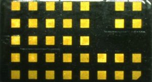
Figure 1, Solder side bottom of the LGA
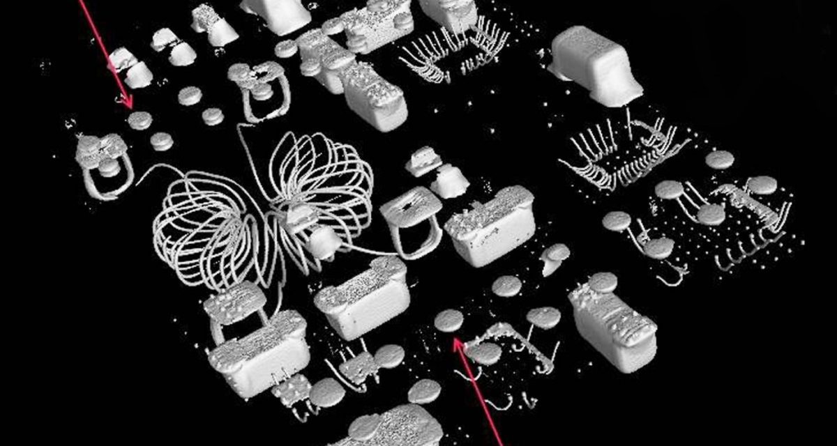
At the Technology Days of the SMTconnect seminar “Soldering”, the process-specific possibilities for reducing the void content in the solder joints of these components to a level of < 10% were presented by Dr. Hans Bell (Rehm Thermal Systems), Henryk Maschotta (Thales Deutschland GmbH) and Dr.-Ing. Heinz Wohlrabe (TU Dresden). Some of the important influencing factors were also presented. For the investigations, modules were available that were equipped with LGA32 and LGA35 (Fig. 1), among others. The internal structure of this LGA and the complex two-sided assembly made X-ray analysis particularly difficult with regard to the robust evaluation of the void content in the solder joints (Fig. 2).
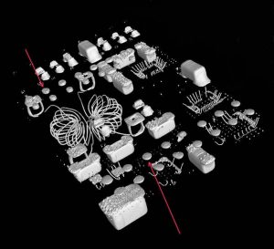
Figure 2, CT image of the soldered LGA internal structure
Within the scope of the project, various X-ray methods (2D-X-Ray, laminography, X-ray CT) were used for comparative purposes in order to obtain evaluable data. In addition to the variations of the PCB design and the material parameters, the final vacuum pressure has been the overall influencing factor on the minimization of the void content (Fig. 3). With decreasing pressure in the environment of the molten solder joints, their void content decreases significantly.
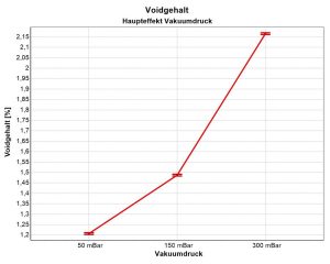
Figure 3, Influence of the final vacuum pressure on the pore content
In general, good LGA solder joints could be produced. The solder wetting of both the LGA connections and the PCB pads was uncritical, as the metallographic investigations prove. The solder gap characteristics essentially correspond to theoretical expectations and the variance is more influenced by the design of the PCB pads than by the voids. The microsections produced reveal the details of the topography of both joining partners, the printed circuit board and the LGA.
Figure 4 shows a section of an LGA32 solder joint in darkfield contrast on which the dimensions of the respective solder resist masks and the gap remaining between them are dimensioned. Only these remaining 13 µm allow the LGA to float in (self-centering) during soldering. Tolerances in the general manufacturing process can further shrink this gap so that both solder resist masks lie on top of each other, making it impossible for the LGA to self-centering.
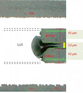
Figure 4, Dark field image of an LGA solder joint
(Photos: Rehm Thermal Systems).


