Advanced Packaging is the Heart of Innovation, According to Yole’s Favier Shoo
By Pradeep Chakraborty
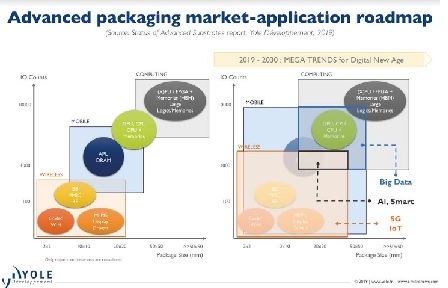
Advanced packaging is said to be at the heart of innovation. Favier Shoo, Technology and Market Analyst in the Semiconductor & Software division at Yole Développement, member of Yole Group of Companies, France, and currently based in Singapore, elaborated: “In the mega-trend driven era of the new digital age, there are key market demands, such as increased I/O and package size overlaps. Low-power consumption also requires packaging innovation and is demanded by many end-applications — from IoT to datacenters.
In order to enable these new performance and functionality requirements, the industry needs a high level of innovation for disruptive technological breakthrough.”
Savior of semicon development
How has advanced packaging emerged as the savior of future semiconductor development? According to Shoo, the main driver in the semiconductor market is changing from mobile to more scattered applications in the future – IoT, automotive, 5G, AR/VR, AI.

Advanced nodes no longer bring the desired cost-benefit, so R&D investment in new lithography solutions and devices below 10nm nodes is rising substantially.
Advanced packaging, therefore, represents an opportunity to increase product value (higher performance at lower cost) offering advantages down both the scaling and functional roadmaps.
New developments in FO landscape
Now, let’s focus on significant new developments in the Fan-Out (FO) landscape. In the core Fan Out (FO) market, the existing players are expected to go compete on cost — between wafer-level vs. panel-level solutions. PTI has commenced Fan Out panel-level packaging (FOPLP) production in 2018, and has made huge investment for this (> 1 billion US$).
Within OSATs, the player who can first satisfy new application demands for mobile and automotive will lead the way, set new standards, and capture the market. In the HD FO market, high-end (mobile APEs) and high-performance (HPCs/networking) is still led by the only significant player, TSMC.

SEMCO has started high-volume manufacturing (HVM) by FOPLP for its Samsung Galaxy smartwatch. Inevitably, the HD FO battle stage is set up for TSMC and SEMCO/Samsung Electronics.
Fan-Out packaging: As the die size scales, reducing ball pitch to have more connections within the die surface may not be the ideal roadmap for chip performance. Hence, the adoption of Fan-Out level packaging.
Fan-Out can integrate dies flexibly at reduced thickness because it eliminates IC Substrate process while also cutting the cost. In short, Fan-Out packaging provides benefits in form-factor, electrical performance and SiP integration capability.
3D TSV/hybrid bonding: TSV, hybrid bonding, or a combination of the two, are the mainstream packaging technologies that are able to provide high-end performance at the integration level reached by the actual stacking technologies.
Huge demand for HBM2 memory: HBM2 has become standard for high bandwidth memory. With 2 main current players in market, Samsung Electronics and SK Hynix, Micron is set to enter HBM business in 2020. Development for the 3rd generation is still ongoing and we can expect much improved performance from this device.
Reshaping automotive packaging
Next, will infotainment, ADAS and electrification reshape the automotive packaging industry as expected?
Shoo added: “Currently, there are two big trends for vehicles, automation and electrification. The trend toward fully autonomous cars has started. We already have level 3 cars on the road now and it will keep evolving. This is changing the automotive electronics landscape.
The impact of electrification should be limited in the next 5 years but, in the long term, the story is different.
Together with more autonomy and future 5G deployment, a third main trend will appear: More connectivity, both internally (infotainment, in-cabin sensors, etc.) and externally (autonomy, safety, 5G facilities, etc.).
Memory back-end manufacturing
On another note, who stands to benefit the most from memory back-end manufacturing? He said: “NAND and DRAM account for ≈97 percent of the overall stand-alone memory market. NAND and DRAM markets are fueled by the growing need for memory in mobile devices (smartphone and tablet) and data centers (storage and memory).
“The combined revenue of NAND and DRAM was up 26 percent from 2017 to 2018. This is a new record for the industry. Samsung, SK Hynix, Intel and Micron are the key players to benefit from this.
“Unquestionably, China has also been investing for long in its domestic IC industry. It has lured various multinational chipmakers to build memory and foundry fabs in China.”
Fan-Out packaging vs. others
Will Fan-Out packaging put flip-chip and advanced substrate manufacturers out of business? Now, HD FO gains market share from the same segment as advanced substrate/Flip Chip, and so is competition.
This trend may continue depending on the extent of Apple, TSMC, Qualcomm and Samsung’s adoption of HD FO in the coming years. For very large package size with huge I/O counts, FO on substrate may be a possible alternative to 2.5D interposers.
In this case, both HD FO and advanced substrate can co-exist without competing. But, as a result, FO on substrate will displace the 2.5D interposers instead.
Key takeaways
Finally, what are the key takeaways for the following segments: AI and HPC, memory and computing, transportation, 5G and consumer?
Favien Shoo noted: “In an evidently smarter world of AI, HPC is the key ingredient for advanced packaging which makes it a mandatory field to investigate and cover. AI and HPC is the new high-end market segment for advanced packaging, making them a mandatory field to investigate and cover.
“Undoubtedly, innovation in memory with HBM and 3D NAND is opening a new field for back-end and packaging with TSV, hybrid bonding in stacking.
5G sub 6GHz require incremental innovation in packaging with small BOM increase, while mmWave requires disruptive innovation. Antenna technology and placement are two of the most critical challenges for 5G semiconductor systems. In addition, a lot of things are happening in China, driven by domestic data traffic, including the deployment of 5G base stations.
In the consumer market, out of the 3 billion device units in entertainment, IoT, Computing, wearables and mobile, close to 2 billion units are from mobile. The mobile market is highly significant and has been the market driver since the end of the PC era. Now, with 5G up and coming, more challenges and opportunities await.