What’s the difference between DFM and DRC?
Or, why do we need Design for Manufacturing (DFM) if we already follow the Design Rule Checking (DRC)?
By Susan Kayesar, Siemens Digital Industries Software
 Customers increasingly ask us why they should run DFM analysis if DRC is already embedded in their design tool. In the quest to help designers create better designs, we have realized that that this basic principle is not always well understood, so we set out to clarify once and for all what the difference is between DRC and DFM and why you truly need both in the PCB design paradigm.
In engineering, design rule checking (DRC) ensures that PCB layout accurately reflects the connectivity and dimensional tolerances defined in the board schematic. The rules mostly define the minimum spacing allowed between various PCB objects for the entire PCB or for individual layers, nets, or areas on the PCB. For designers, the spacing may affect circuit performance. For manufacturers, spacing affects the ability to fabricate or assemble the PCB.
Design for manufacturability (DFM) is the process of arranging a PCB layout topology in a way that mitigates problems which could be encountered during board fabrication and assembly. In casual terms, just because you can create a certain design doesn’t mean that you should, or that it is practical, cost-effective, or reliable to produce. DFM addresses the “should” aspect, whereas DRC addresses the “can.” Specifically addressing fabrication issues is called design for fabrication (DFF) and focusing on assembly issues during design is referred to as design for assembly (DFA). Combined they make up the DFM analysis process.
Designers often rely on their manufacturer to run DFM checks on their designs, trusting the manufacturer to work through most issues on their own and report back only those issues that absolutely necessitate a design revision. This standard process can cause significant delays and leaves the quality, yield, and price entirely up to the manufacturer to determine. Performing DFM in-house before handoff can save time, and you can retain ownership of critical design parameters that affect price and quality. So why is in-house DFM analysis not always a required and standard part of the design to manufacture workflow? There are several common misconceptions about DFM that may prevent designers from adopting it into their workflow.
The first common mistake designers make with regards to DFM is to think of it as a testing checklist that occurs outside of the design process. Instead, DFM should be performed as early as possible and as often as practical during layout. Integrating DFM early in the design phase empowers designers to avoid design faults before they become enmeshed in the PCB layout and difficult to resolve. As PCBs become more complex, DFM should be used as design guidance rather than a laundry list of fixes to be made after the main work is finished. Running DFM checks in addition to adherence to DRC gives designers early insight into issues that could be encountered much later in the product lifecycle and enables them to bypass those issues with intelligent design.
Another common misconception is that adding DFM to the layout phase is a time-consuming and expensive addition to DRC. The legacy workflow of handing off a design to manufacture and waiting for DFM results to dictate and clarify changes, reworking the design and handing off again until the manufacturing criteria are met, serves only to perpetuate this myth. Performing DFM in-house before handoff saves significant time by eliminating the extra wait time between iterations, and the design can arrive in the manufacturer’s inbox ready for final approval and production.
The software cost of in-house DFM is offset by the time and resources saved by eliminating respins, and new online DFM offerings, such as Siemens PCBflow, are now available, which lowers the cost further and provides pay-per-use models that are often more cost-effective for smaller businesses.
An additional misstep is leaving identification and resolution of design faults to the manufacturer, often due to the belief that it is difficult to identify the critical issues. In the past, DFM value may have been lost by providing too much information and failing to offer a way to filter through and easily flag the most important flaws. Traditionally it has been difficult for a designer to guess what the manufacturer will specify as their top DFM concern because manufacturing engineering requires skill and knowledge of chemical and mechanical processes beyond the scope of most designers’ role.
However, industry has pushed DFM to adapt to new complexity levels, and today’s discerning designer can find a DFM solution that offers clearer, more focused findings and gives actionable information to resolve violations. Enhanced collaboration empowers manufacturers to clearly communicate their specific limitations and requirements, and designers can now employ tailored DFM to anticipate and address manufacturability concerns with their preferred manufacturer.
Industry 4.0 is speeding up the design-to-market lifecycle, and designers are pressured by strict timelines for product release. In today’s marketplace, it can be tempting to send a design to manufacture before it is fully analyzed and optimized, if analysis is deferred to the last stage before handoff. When discussing the difference between DRC and DFM, remember that faults uncovered by DFM (vs. DRC) may not always appear in a single or low-volume prototype. However, as volume is increased, preventable quality and yield issues will become apparent for designs that have not undergone DFM analysis. Thankfully, Industry 4.0 is also providing new tools for communication and efficiency and opening virtual collaboration spaces. Quicker, more accessible DFM is part of that revolution.
Integrating in-house DFM analysis is already common practice for enterprise companies. Using powerful on-premises solutions affords enterprise companies the luxury and convenience of reducing project duration, mitigating risk, increasing yield and generally getting to market faster and with confidence. Large companies often have technologists on hand to coach designers through the DFM process and provide ongoing advice about manufacturing technology. Smaller businesses tend to shy away from what they see as a high-end product priced out of reach. They are unnecessarily deterred from performing DFM and make do with whatever DRC is available through their design tool.
To address the needs of these small and medium-sized businesses, Siemens introduced PCBflow. This new solution provides an online subscription-based DFM solution powered by the Valor NPI engine and fueled by real-world manufacturer defined DFM rules. With free registration and membership, a unique collaboration opportunity is provided in PCBflow. Using this option, designers can implement DFM on an as-needed basis and harness the power of the community to network with manufacturers, essentially bringing the market to the design as well as the design to the market.
Our Case Study
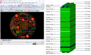
Researchers at a Siemens R&D facility in Munich ran different PCB designs through the PCBflow tool. The following is an illustrative description of their first use of PCBflow for a control PCB, which is the central controlling unit in a system with many sensors and mechanical components. Because of space limitations within the system, the circuit board contour is round with a 70.5-mm diameter. On this small disk, 550 components with 2,838 pins must be placed on both sides. To route this many components, which consists of a mixture of fine pitch active devices (ball grid array down to 0.5-mm pitch) and small passives (down to 0201 package size), a high-density board (HDI) construction was mandatory. The board design was made with the Xpedition layout system.
Figure 1 shows the placement of the components and the board construction. The board consists of an eight-layer core with one sequential buildup layer on each side. The connection between top and bottom layer to the core is with blind vias. Buried vias connect the different inner layers within the core.

Figure 1. Control PCB: Placement of 550 components on top and bottom side (left) and 10-layer board stack up (right).
They validated the PCB design against a DFM profile before sending the data out to a PCB supplier. They uploaded the design, which was saved as an ODB++ compressed file, to the PCBflow service and selected a DFM profile of a preferred PCB manufacturer. The manufacturer dashboard displays the company and location as well as the name and status of the DFM profile. Profiles with the status “public” are available to all users. Profiles with the status “limited” belong to companies that we are connected to within the PCBflow network.
The next step was to click the RUN DFM button to start the analysis process. Once the DFM analysis progress bar reached 100%, the DFM report was presented automatically. The complete analysis for this complex HDI board took only 90 seconds.
The DFM report shown in Figure 2 is interactive and allows filtering as well as scrolling options. The DFM report consists of two panes. The information pane contains general information about the board as well as error statistics derived from the ODB++design data. The results pane displays the analysis results as a tree and provides controls for viewing and exporting the results.

Figure 2. DFM report with information pane (left) and analysis results per layer (right).
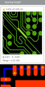
The DFM check of the control PCB identified a set of issues that could create problems during the production or assembly of the boards. First, they saw a reduced copper spacing over a long distance between two tracks was reported on signal layer 3. Detailed information such as actual value (3.416 x 61.245 mil) and the x,y location of the error is provided (Figure 3 top). They appreciated being able to see a description of the constraint when pushing the information button. According to the constraint tolerance range, the severity is assessed “yellow = warning.” This informed them that the PCB manufacturer could have severe yield issues caused by electrical short circuits unless the distance between the tracks is enhanced. The DFM analysis detected several unwanted stubs on the outer layers (Figure 3 bottom).

Figure 3. Top: Spacing length issue as reported in the DFM report. Bottom: Copper stubs on outer layers.
Because the distance between the adjacent copper structures is larger than the value set in the design rule check (DRC), those routing artifacts were not recognized during the layout of the board. And, because the pitch of the SMD pads is only 0.5 mm, those copper “noses” can result in solder bridges during assembly of the components. As a result, they removed all reported copper stubs.
Several warnings for stubbed vias were also reported. Buried vias between layer 2 and 9 of the core were only connected on one side. Those vias are useless, can cause a significant signal degradation and lead to higher drilling cost. They could improve the quality of our design by removing those buried vias.
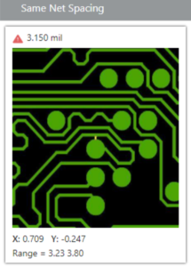
A violation against the constraint “same net spacing” was reported on layer 3 (Figure 4). The small space between copper structures of the same net creates an acid trap. An acid trap has the potential to trap chemical etchants used to strip excess copper from a board during the manufacturing process. When the etching solution pools in a certain area, there is a risk for corrosion of traces and creation of faulty connections or open circuits. So they changed the routing, keeping in mind the length matching requirement.

Figure 4. Constraint “same net spacing.”
The researchers’ experience with running DFM analysis on this board, and many other experiments, in PCBflow, illustrated that they could improve the design in a very short time without any interaction with the PCB manufacturer during the layout phase.
In conclusion, we have seen that adding DFM to your current DRC checks is a value and quality proposition. This process is now readily available to all designers and should not be forgone due to common misconceptions about price, time, or difficulty.
Author Bio
Susan Kayesar is a PCBflow Product Manager for Siemens Digital Industries Software. She holds a BSc from Tel Aviv University and brings over 20 years of experience in the PCB design and verification industry. She is an expert at cultivating creative software solutions to meet real-world customer needs, and, in the past, has provided support, training, and consultancy services for both simple and complex product implementations. In her spare time, Susan enjoys travel, hiking, and coffee.


