Cloud-Based DFM Enables Real-Time Collaboration between PCB Manufacturers and Designers
By Oren Manor, Director of Business Development, Valor, Siemens Software
Listen to the webinar on this topic by registering here>>

Oren Manor
The electronics industry has been trying to shift design for manufacturing (DFM) further upstream in the product production process with variations in success, but for this practice to be successful, design engineers and manufacturers must be willing and able to collaborate.
Even when designers are provided with the best-in-class DFM applications, a primary obstacle to shifting DFM checking to the left is often the reluctance for manufacturers to be as transparent as needed. Suppliers also are often not readily willing to cooperate despite all the benefits, because of IP ownership and security issues.
Even when done entirely in-house, product design in traditionally is separate and isolated from the manufacturing process. This siloing often results in one-to-several redesigns to make the product manufacturable, adding time and cost to the project. This results in only partial manufacturing needs taken into consideration early in the design process. The fallout means many technical queries, inefficient data exchange, and avoidable revision spins.

One of the biggest challenges in the process of a design to manufacturing handoff is the lack of manufacturing knowledge and data while still in the design phase. Often, there is no communication between designers and manufacturers. The manufacturing process changes, and manufacturers buy new machines. They also learn from mistakes and adapt their manufacturing constraints. Oftentimes, the designer does not get these updates, and then over time, their “local” constraint file becomes less relevant to the actual manufacture process.
Handoff to manufacturing typically is managed by the procurement department.
Procurement for PCB fabrication is important, but it also crucial that the PCB design can be manufactured by the fabricator. Without direct communication between the designer and fabricator during the design stage, the designer finds out that the product does not comply with the manufacturer’s constraints, or a fabricator discovers that they are unable to fabricate it, late in the process.
Design companies and OEMs contract new manufacturers frequently. In 2020, this practice accelerated because it has become critical to include local suppliers because of travel restrictions. Developing a new constraint set for a new supplier is challenging. Supplier business-to-business (B2B) networks use various communication methods to exchange data between buyers and suppliers: emails, communication over phone, negotiations, business deals, contracts, quotes, invoices etc. The data exchanged from design to manufacturing needs to be quick but also must be secure.
Secure, Online DFM Analysis Means Products Can be Built Better and Faster
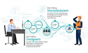
To address these challenges, Valor engineers built Siemens first software-as-a-service (SaaS) solution that combines Valor NPI design-for-manufacturing capabilities with the Mendix app development platform: PCBflow. We have partnered with Amazon Web Services (AWS) to provide a secure online environment where PCB design teams can interact with manufacturers and rapidly perform a range of DFM analyses in the context of each manufacturers’ process capabilities, accelerating design-to-production handoff.
Software as a service (SaaS) eliminates the need for local client software installation and configurations. These cloud solutions should incorporate strict security standards, reducing risk and protecting intellectual property (IP) for companies and individuals to use them with confidence and assurance in their data protection. SaaS technology reduces risk and protects intellectual property with no additional IT investment. The Mendix platform provides the ability to build multi-experience apps and share data from any location, on any device, on any cloud or platform, to realize the benefits of digital transformation more quickly.
PCBflow incorporates the strict security standards of Siemens software and the AWS cloud so that manufacturers can feel safe with their manufacturing constraints, and designers feel safe running DFM analysis for their designs. With PCBflow, both parties can be confident working together in a secure cloud environment.
Security and IP protection is assured because the connection requires approval of both sides and each party only has access to its data. Meaning designers can only view their design but not manufacturing constraints and manufacturers can see their constraints but not the PCB design. Once a connection is established by the request’s recipient, PCBflow collaboration is enabled between the two parties. Manufacturers can upload and allow known customers to “connect” share their advanced manufacturing rules with their approved designer network.
Through PCBflow, designers and manufacturers can communicate directly and exactly how they need to for exchanging information. By collaborating at an early stage, the design can be validated against the manufacturer’s specific constraints, accelerating the handoff process to manufacturing.
For the manufacturer, when a board is released, it often has issues with the design that can negatively affect yield. Asking the designers to correct the issues usually involves lengthy phone calls or emails, which costs time. With PCBflow, fabrication capabilities are communicated electronically, and are always up to date allowing the design team to design directly to your requirements. Customer access to the manufacturing process capabilities is controlled and secure. The result of design executed DFM based on fabrication capabilities means fewer callbacks and higher yield.
With manufacturing-specific capabilities built into PCBflow, designers can ensure manufacturability, saving time. Manufacturers control who is allowed run the analysis based on their profile. Providing manufacturing knowledge to designers builds teamwork and collaboration, which results in fewer callbacks. Customer access to process capabilities is controlled and secure. With PCBflow, manufacturing capabilities can be provided to an expanded audience, increasing the conversion rate of new customers.
Business Case
Nistec is a leading provider of electronic design and manufacturing services. It is comprised of four companies that together provide full service from design to the final product including layout, manufacture, and assembly services for various industries, including communication, medical, military, security, industrial, and vehicles. Nistec Design Bureau is the largest of its kind in Israel and has 22 designers.
Designing a PCB is a highly complex process that includes thousands of decisions, each of which can be critical and lead to an error. Losses can add up significantly if a mistake is revealed after the manufacturer already purchased the components, if engineering hours were invested for vein, or if manufacturing is completed and the product is not working. To prevent that, Nistec designers run a manual internal check on the PCB design before sharing it with their manufacturing division. Checking all aspects of the design’s manufacturability by hand is extremely challenging and time-consuming.
With dozens of new product introductions (NPIs) per month, time and efficiency are critical to getting their customers’ products out the door. The design/editor must define the manufacturability constraints per each job, which may differ from job to job. These preliminary definitions are crucial for the success of the production. Nistec wanted to improve their response time while maintaining their high-quality work.
They chose the new PCBflow (while it was still in its beta development stage) to help them in the process of evaluating their design and improving on it. Nistec CTO, Evgeny Makhline, worked closely with PCBflow Product Manager, Yossy Pinhas. Makhline ran tens of checks with PCBflow, and then shared his feedback with Pinhas, especially pointing out the most important parameters that PCBflow should cover.

For a DFM tool, they depended on an external partner who owns the solution, so it is not available constantly for Nistec. Until now, Nistec designers had been using a DFM flow mainly for their most complex designs. Thanks to PCBflow’s ability to incorporate specific manufacturing knowledge for a selected manufacturer, shifting checks left into the design process becomes an automated comprehensive process. This reduces the potential for mistakes and increases PCB design quality significantly.
“PCBflow is a great solution, a win-win for board and layout designers and for fabricators. On one hand, layout designers get easy access to a cost-effective, easy-to-use platform that quickly identifies design issues and constraint violations that could affect manufacturability, and then connects them with a wide variety of fabricators. The fabs, on the other hand, receive a ‘mature’ design that requires little or no review or troubleshooting – a big saving in time and improvement of quality,” said Makhline.
Usually, with an on-premise DFM tool, the actual analysis would take three hours. Then, the iterations when communicating manufacturing requirements to the designer could take between one to three days. With PCBflow used on their simple and/or complicated designs in house, it takes one minute to generate the analysis report. Thanks to this solution, Nistec intends to promise its customers a shorter time to market while ensuring the highest quality.


