XRF: a Powerful Tool for Electronics Quality, Counterfeit Prevention, Compliance
By Mark Northrup, Nabahe “Bo” Tewawina, IEC Electronics and Ralph Dalfonso, Delta Sales
X-Ray Fluorescence (XRF) is a fast and accurate analytical technique that uses x-rays’ interaction with a material to determine its elemental composition. It is a non-destructive test that can be applied to the analysis of solids, liquids and powders. XRF is also the method of choice for determining the thickness and composition of coatings.
XRF spectrometers range from hand-held devices to benchtop systems designed for processing large and multi-part (and multi-spot) sample configurations.

Mark Northrup
There are two main XRF methodologies: energy dispersive (EDXRF) and wavelength dispersive (WDXRF). Both analyzers use an x-ray source to excite the sample With WDXRF, X-rays with wavelengths characteristic of the elements in the sample are emitted, and they, along with scattered source x-rays, move in all directions. A crystal or other diffraction device is positioned in the path of the x-rays that are diffracted and scattered from the crystal. Depending on the spacing between the atoms of the crystal lattice and their angle in relation to the sample and detector, specific wavelengths directed at the detector can be controlled.
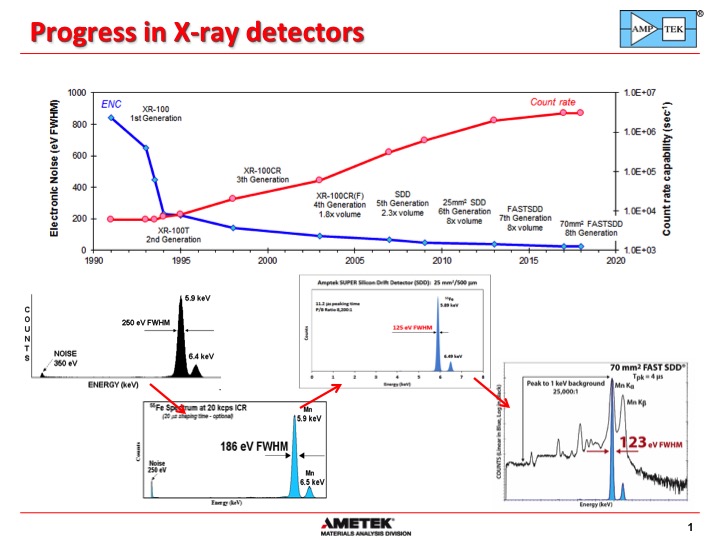
EDXRFs have several unique and notable capabilities, thanks to recent improvements in detectors and optics. In the beginning, proportional (“prop”) counters were XRF’s detection method. These gaseous ionization devices measure the energy of incident radiation by producing a detector output proportional to the radiation energy. Prop counters are still well-suited to the measurement of single-layer deposits, and simple applications where baseline noise is not a factor.
The complexity of today’s PCB fabrication, electrical components and cable connectors, however, has made this XRF detection method obsolete for the builders of printed circuit assemblies. Most are now required to use the higher technology XRF detector alternatives, Silicon PIN Diode and Silicon Drift Detectors.
Silicon PIN Diode provides spectral resolution superior to proportional counters, so technicians can measure thinner deposits and lower element concentrations, and perform more complex measurements, such as those involving alloys and multiple-layer samples. The “gold standard” for XRF instruments using Silicon PIN Diode technology will precisely measure up to 5 coating layers, some or all of which can be alloys. This is a huge advantage for ENIG/ENEPIG/EPIG processing.
Silicon Drift Detectors (SDDs) are the hands-down choice for films below 50 µm, and complex films such as those used throughout the tech sector. They generate the highest count rates, which is key to achieving a low minimum detection limit (MDL), and produce the highest spectral resolution – typically 50% higher than silicon PINs.
SDDs offer significant peak-to-background ratio improvement compared to prop counters. They also have the lowest baseline noise and the widest element testing range. For greatest usability now and in the future, the element range for companies in the electronics arena should span from Aluminum (13) to Uranium (92.)
Because they are the champs at filtering noise, SDDs are the most effective for quantifying overlapping elements – positions on the periodic chart where there is minimal separation of signals between elements (nickel, copper, zinc, chrome, iron, for example). With older XRF systems, it’s impossible to resolve overlapping elements without manual math. The resolution provided by both silicon PINs and SDDs makes this post-test calculating task obsolete.
The other differentiator that merits attention is optics. Just as prop counters were the starter technology for XRF detection, pin hole collimators provided the training wheels for early XRF optics. Entry-level XRF systems still use collimators, but where precision is the priority, polycapillary optics, such as what’s used in Bowman XRF systems, delivers the ultimate enhancement to XRF measurement performance.
The concept here is that the x-ray source, on its own, is incapable of producing a high-density beam. Polycapillary optics focuses the beam, as opposed to pin-holing it to its target.
Faster speeds – a “high-desirable” in electronics – are enabled by a smaller x-ray beam and a flux fully 100x higher than a collimator. The higher flux allows more photons to be counted, thereby delivering the most precise results.
Polyoptics also delivers a cleaner excitation beam than is possible with a collimator, because there’s no pinhole scatter and the focus location is well-defined.
PCBs and XRF
Recently, IPC*, the global source for electronics industry standards, training, and public policy advocacy, issued its long-awaited standard, IPC 4552-Rev. A. The release presents a challenge for printed circuit board manufacturers that apply ENIG / ENEPIG / EPIG coatings to their printed board assemblies because it assigns an upper limit on the amount of gold that is applied. As a result, gold thicknesses must be closely monitored. To accurately measure gold thickness:
- Gold (Au): 0.04-0.1µm (1.58-3.94µin) with a +/- 3 sigma standard deviation applied
- Nickel (Ni): 3-6µm (118.1-236.2µin)
Shops that plate advanced finishes also need to precisely quantify both phosphorus and electroless nickel, tasks only possible with a Silicon Drift Detector.
This 4552-A standard requires specific XRF hardware, software, and calibration protocols. Many PCB manufacturers already use XRF equipment as part of their quality control process, but have discovered that most older instruments cannot meet the new IPC specifications, and an upgrade to newer XRF technology will be needed.
Counterfeit EEE Components and XRF
SAE AS6171/3 recognizes that X-ray Fluorescence Spectroscopy is effective for evaluating electrical, electronic, and electromechanical parts. Parts removed from a circuit board may have material contamination from the assembly, making the use and removal process worth considering when using XRF detection results for counterfeit analysis.
Counterfeit components risk mitigation is based on the identification of elements (or absence thereof) in specific locations on or within a component. XRF is useful for counterfeit components detection on the external surfaces of as-received components, and on de-lidded, de-capsulated, or otherwise prepared components. The indication of counterfeit components can also be based on the concentration levels of materials under consideration and thicknesses of the material layers. For reliable decision-making, XRF analysis is compared to known results based on manufacturer specifications. In the absence of manufacturer references, XRF analysis can be used to compare component-to-component consistency within a date code lot.
RoHS and XRF
XRF systems are used worldwide to test products for RoHS compliance, a critical factor that now affects every company manufacturing in, or selling to, the 28 countries of the European Union and the three others that impose RoHs standards.
RoHS 1 stands for Restriction of Hazardous Substances. RoHS, also known as Directive 2002/95/EC, originated in the European Union and restricts the use of specific hazardous materials found in electrical and electronic products. Applicable products in the EU after July 1, 2006 are required to be RoHS compliant. The worldwide RoHS, WEEE and ELV directives specify strict limits on the use of lead (Pb), mercury (Hg), cadmium (Cd), hex chromium (CrVI), polybrominated biphenyls (PBB), polybrominated diphenyl ethers (PBDE), and four different phthalates in materials used to manufacture automotive components and consumer electrical goods.
RoHS 2, or the Recast RoHS 2 Directive 2011/65/EU, was published in July 2011. The scope of the original RoHS was expanded to cover all electrical/electronic equipment, cables, and spare parts, with compliance required by July 22, 2019 or sooner depending on product category. RoHS 2 is also a CE-marking directive, with RoHS compliance now required for CE product marking. As such, all manufacturers of electrical/electronic products must comply with RoHS 2 before the CE mark can be applied to their products.
The original green RoHS label with the checkmark is no longer used, as RoHs compliance is now integral to the CE mark. RoHS 3, or Directive 2015/863 was published in 2015, and adds four additional restricted substances to the original list of six.
On the other side of the Atlantic, the US Consumer Product Safety Commission (CPSC) has acknowledged XRF as a valuable tool for detecting heavy metals and other hazardous materials.
Conclusion
The challenges of RoHS, counterfeit parts, and new PCB finishes make a compelling case for the adoption of current-day XRF technology. There is also, of course, the economics issue: precision XRF systems assure that plating deposits meet specification, avoiding rejects (for under-plating) and unnecessary, unrecoverable costs (for over-plating).
* IPC – Association Connecting Electronics Industries®
If you have feedback or suggestions, or want to contribute to the advancement of XRF measurement technology in PBAs, please contact Nabahe, Ralph or myself.
Nabahe “Bo” Tewawina
Laboratory Lead
Mark Northrup Ralph Dalfonso
IEC Electronics Delta Sales
mnorthru@iec-electronics.com rdalfonso@dsareps.com